Key answers
- Why this device matters
- Germanium absorbs telecom-band light while remaining compatible with silicon-photonics integration. Virot and co-workers demonstrated a lateral double Si/Ge/Si heterojunction photodiode with contacts on silicon, reporting less than 10 nA dark current, more than 1.1…
- What the model calculates
- The package combines a generic multi-layer layout with a transparent reduced-order model. It calculates:
- What the GDS represents
- The generated cell GE_PIN_LATERAL_CARTOON_VIROT_CLASS is a top-view engineering cartoon: optical guide, rectangular Ge region, separate silicon-side p/n regions, vias, metals, and labels. Its layer numbers are project-local visualization layers. It does not encode a…
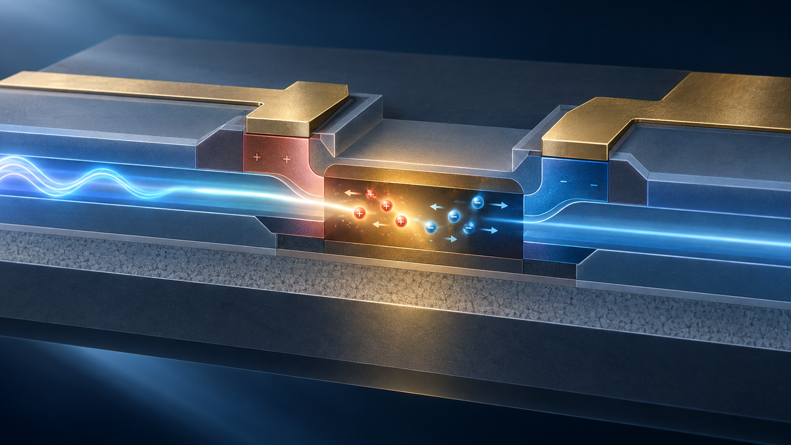
A transparent engineering model for a lateral Si/Ge/Si PIN photodiode
High-speed photodetectors are a practical bottleneck in silicon-photonic links: they turn modulated light into an electrical current that the receiver can amplify and decode. This new open-source project adds a lateral silicon/germanium/silicon PIN photodiode budget to the PhotoBattery device library.
Method estimate from assumed inputs. The numerical results below are not measurements, foundry specifications, or reproductions of published devices.
Why this device matters
Germanium absorbs telecom-band light while remaining compatible with silicon-photonics integration. Virot and co-workers demonstrated a lateral double Si/Ge/Si heterojunction photodiode with contacts on silicon, reporting less than 10 nA dark current, more than 1.1 A/W responsivity, and more than 50 GHz bandwidth at -1 V. Lischke and co-workers later reported a different biconcave germanium-fin architecture reaching 265 GHz at 1 mA photocurrent. These are separate devices and their measurements must not be mixed into one synthetic preset.
The broader silicon-photonics roadmap identifies communications as a mainstream demand and notes that high-speed germanium photodiodes are native to several foundry platforms. It also highlights the continuing need for better compact models and process design kits.
| Reference device | Reported evidence | Architecture | Qualification for this article |
|---|---|---|---|
| Virot et al. (2017) | >1.1 A/W responsivity, >50 GHz bandwidth, <10 nA dark current at −1 V | Lateral double Si/Ge/Si heterojunction | Measured literature benchmark; not reproduced here |
| Lischke et al. (2021) | 265 GHz 3 dB bandwidth at 1 mA photocurrent | Biconcave germanium fin | Separate measured device; not mixed into the nominal preset |
| This open model | 1.023 A/W responsivity, 45.8 GHz combined bandwidth | Generic lateral Si/Ge/Si engineering cartoon | Reduced-order calculation from stated assumed inputs |
What the model calculates
The package combines a generic multi-layer layout with a transparent reduced-order model. It calculates:
- Beer-Lambert modal absorption from an explicitly assumed effective modal absorption coefficient.
- Responsivity from absorbed fraction and an assumed collection efficiency.
- A parallel-plate lateral-junction capacitance estimate plus a separate assumed parasitic capacitance.
- Electron and hole transit responses from a one-dimensional Ramo-Shockley integration.
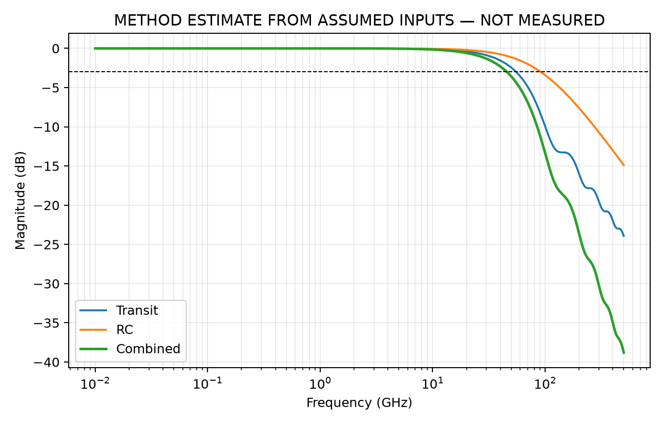
- RC and combined small-signal frequency responses.
- Optional ideal shot and Johnson noise when a measured or process-calibrated dark current is supplied.
The nominal demonstration uses a 20 µm optical length, 0.6 µm carrier transit width, 15 fF assumed parasitic capacitance, 50 Ω assumed diode series resistance, and a 50 Ω instrument load. It produces an absorbed fraction of 0.909, responsivity of 1.023 A/W, parallel-plate capacitance of 2.36 fF, RC bandwidth of 91.7 GHz, transit bandwidth of 55.3 GHz, and combined bandwidth of 45.8 GHz. Because the operating bias is unspecified, the transit result is labeled a high-field ceiling.
Here, Aabs is the modeled absorbed fraction and ηq is the assumed collection efficiency. The equation exposes the assumptions rather than presenting the result as a measurement.
What the GDS represents
The generated cell GE_PIN_LATERAL_CARTOON_VIROT_CLASS is a top-view engineering cartoon: optical guide, rectangular Ge region, separate silicon-side p/n regions, vias, metals, and labels. Its layer numbers are project-local visualization layers. It does not encode a foundry layer map, implant dose, Ge recess or seed, silicide enclosure, GSG pads, or sign-off design rules.
The automated topology checks verify that the p-side and n-side metals remain separate and that required shapes are present. KLayout then writes and reads the GDS to verify round-trip integrity.
Reproduce the result
The complete source, tests, CSV data, plot, and generic GDS are available in the immutable open-source project release on GitHub.
The visually verified two-page engineering note is available as a PDF.
git clone https://github.com/ShahramPhotonics/silicon-photonics-eda-portfolio.git
cd silicon-photonics-eda-portfolio/51-ge-pin-photodiode
python -m venv .venv
source .venv/bin/activate
pip install -r requirements.txt
python run_analysis.py --out results
pytest -q tests
The release passed 15 targeted tests and the portfolio-wide verifier for all 51 projects. Those checks cover analytic limits, charge conservation at midpoint and edge birth, frequency roll-off, capacitance scaling, resistance and velocity sensitivity, invalid inputs, metal topology, and KLayout round trip.
Limits and the next validation step
This is an educational engineering budget. It is not TCAD, a full-wave optical calculation, measured silicon, a PDK cell, or a tape-out-ready layout. The largest uncertainty is the assumed effective modal absorption coefficient and collection efficiency. The capacitance model omits fringing fields, mixed Si/Ge dielectric behavior, depletion-voltage dependence, pads, and package interconnects.
For a real design, replace every assumed input with values from one internally consistent measured device or calibrated solver. Then compare the predicted responsivity and S-parameter bandwidth against that same device before changing geometry.
Primary sources
- L. Virot et al., “Integrated waveguide PIN photodiodes exploiting lateral Si/Ge/Si heterojunction,” *Optics Express* 25, 19487–19496 (2017). Supports the measured lateral-device benchmark.
- S. Lischke et al., “Ultra-fast germanium photodiode with 3-dB bandwidth of 265 GHz,” *Nature Photonics* 15, 925–931 (2021). Supports the distinct biconcave-fin benchmark.
- S. Shekhar et al., “Roadmapping the next generation of silicon photonics,” *Nature Communications* 15, 751 (2024). Supports the platform and compact-model context.

Leave a Reply